HJCBUG 《微型计算机》 2010年3月上期
制程的历史与演进
CPU制程技术发展到今天,其尺寸已经从1971年Intel发布的4004 CPU时的10μm进化到了今天的32nm级别,Intel公司最新推出的新款处理器—代号Westmere的32nm制程处理器(见图1)就是目前顶尖制程工艺的代表。台积电也计划于年内推出其28nm制程工艺,另外一家主要的芯片制造厂商GlobalFoundries公司则计划于年内推出基于SOI的32nm制程工艺和基于体硅的28nm制程工艺。
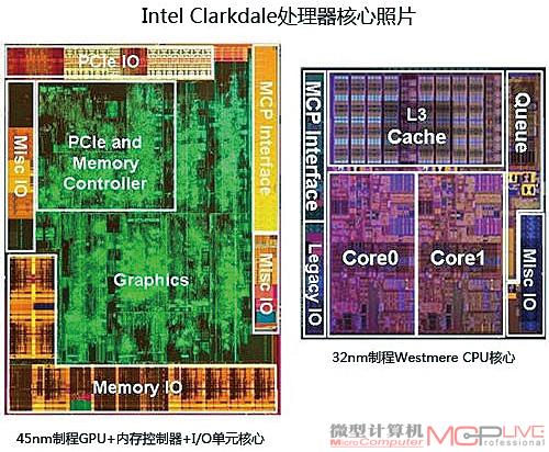
图1:45nm制程和32nm制程
不过,从早期的Intel 486时代发展到目前的Westmere,各家厂商制造CPU的制程基本都是基于传统的平面型晶体管结构,熟悉 MOSFET结构的爱好者都知道,所谓的平面型晶体管,指的是MOSFET的漏极、源极、栅极、沟道以及基体结构的横断面位于同一平面上的晶体管结构,如图2所示:
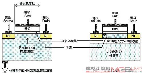
图2
需要说明的是,即便是传统的平面型晶体管技术,业界也存在两种不同的流派,上图中左侧的称为传统的体硅技术(Bulk SI),而右侧的则是相对较新的绝缘层覆硅(SOI)技术,两者的区别在于后者在硅基体顶部增加了一层埋入式氧化物(BOX)层,而BOX上则覆有一层相对较薄的硅层。Intel是体硅技术的坚定支持者,而IBM/AMD则是SOI技术的绝对守护者。
尽管历经了数十年风雨的平面型晶体管制造技术发展至今已经相当的成熟,对各家厂商而言也是最经济的制造技术,但随着晶体管关键尺寸的不断缩小,平面型晶体管技术的瓶颈现象越来越严重。那么是在现有的部分耗尽型平面晶体管(为了行文方便,下文如不作特别说明均用传统平面型晶体管表示部分耗尽型平面晶体管)技术上进行新技术研究还是抛弃现在的传统平面型晶体管以求创新呢?下面我们就以这两个方向作分别阐述。
延续现有晶体管架构
应变硅与HKMG——延续传统平面型晶体管的希望
在过去的几十年中,为了延续传统平面型晶体管制造技术的寿命,弥补关键尺寸缩小给传统平面型晶体管带来的负面效应,以Intel、台积电、AMD(也就是现在的GlobalFoundries)为代表的制造厂商已经开发出了很多能够改善传统平面型晶体管性能的技术,这些技术中,已经投入商用的技术尤以面向改善沟道性能的应变硅技术和改善栅极性能的HKMG(High-K栅氧化物层+金属栅极,此后简称HKMG)技术为代表,自从Intel在90nm制程的Pentium 4处理器上首次启用应变硅技术之后,这两种主要的辅助技术便成了各家厂商开发制程技术的两大热点,各家厂商均先后在自家制程工艺中加入了类似的技术,Intel和AMD包括台积电都在90~32nm的演进过程中采用了应变硅技术和HKMG技术,尽管他们的具体实现手法不同。为了读者能够更好的理解本文,下面我们就对这两种技术进行简单的介绍。
a.应变硅技术
注意图3中的“启用eSiGe(嵌入式硅锗)材料”,指的便是专门用于改善传统平面型晶体管管沟道性能的应变硅技术中的一种,应变硅技术的实质是改善沟道中空穴/电子流动的速度。
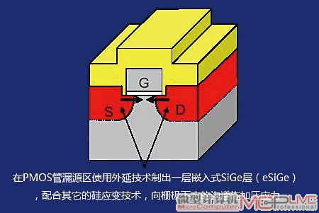
图3
eSiGe技术主要面向PMOS管,其原理是在PMOS管的漏源区外延生长一层晶格常数(即晶格原子之间的距离)比PMOS沟道中硅材料的晶格常数更大的SiGe层,以此来生成对PMOS管沟道压缩应力的技术,其原理如图3所示。根据研究,当向PMOS管沟道施加纵向(即栅极宽度方向)的压缩应力时,可以大大改善沟道的载流子移动性,提升效率。
PMOS是指N型衬底、P沟道,靠空穴的流动运送电流的MOS管,全称为P-channel Metal Oxide Semiconductor FET;NMOS是指P型衬底,N沟道,依靠电子的流动来运行电流的MOS管。全称为N-channel Metal Oxide Semiconductor FET。
b.HKMG技术
HKMG是以High-K绝缘层替代传统的SiO2氧化层,并以金属材料栅极替换旧有的硅材料栅极的一项技术,这项技术主要有助于晶体管开关速度的提升,并可减小栅极的漏电流。我们可以看到,Intel、AMD和台积电都在自己的制程工艺规划中加入了HKMG技术,说明这项技术得到了三巨头的普遍认可。图4是Intel 45nm制程NMOS管的HKMG结构实物图:因为篇幅有限再加上这两个技术点非常复杂,这里就不对应变硅和HKMG进行展开描述了。
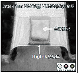
图4
看到这里可能你会问,应变硅和HKMG技术不就可以让传统平面型晶体管一直延续下去了吗?非也,当制程下降到15nm以下后,传统平面型晶体管本身的技术壁垒将成为很难逾越的大山,除非在这段时间内又有新的“奇兵”技术出现。
传统平面型晶体管技术的瓶颈
尽管应变硅和HKMG技术曾经相当有效,而且在过去的一段时间里也起到了成功延续传统平面型晶体管寿命的重要作用,但以栅极宽度为代表的关键尺寸的不断减小所带来的负面效应已经越来越明显。
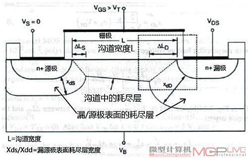
图5
首先,当栅极宽度减小到一定程度后,如图5所示,沟道的宽度(图中的L)也必然随之缩小,此时由于源、漏极区覆盖的耗尽层宽度(图中的XdS和XdD)在整个沟道中所占的比重增大,与沟道耗尽层重合程度也越来越大,这便会导致所谓的短沟道效应(SCE)。
什么是短沟道效应?
随着MOSFET沟道长度不断缩短,使得MOSFET出现了一系列在长沟道模型中得不到反映的现象,而这些原来可以忽略的效应变得愈发显著,甚至成为影响性能的主导因素,这种现象的统称即为短沟道效应。短沟道效应的坏处多多,首先是容易造成栅极门限电压Vt的上升,使管子的功耗增加;其次是可造成热载流子效应,影响器件寿命,另外还有可能造成管子无法关断,沟道中载流子迁移率下降等问题。
为了控制短沟道效应,人们不得不向沟道中掺杂磷、硼等杂质元素,这便导致用于控制管子开关的门限电压Vt的上升,同时还会降低沟道中空穴/电子流动的速度,造成管子速度的下降。而且用来向沟道中掺杂杂质的离子注入工艺也存在很难控制的问题,很容易造成管子门限电压过大等不良结果。其次,传统的SiGe PMOS应变硅技术也开始面临瓶颈,以Intel为例,截至目前为止,其应变硅技术在32nm制程节点中已经发展到了第4代。在Intel的第4代应变硅技术中,PMOS管漏源区内的eSiGe层掺杂的Ge元素比例也已经达到了40%的水平。很难再为沟道提供更高级别的应变。第三,栅极氧化物的厚度方面也将出现发展瓶颈问题。仍以Intel为例,其HKMG技术在32nm制程节点中已经发展到了第二代,其第二代HKMG技术中High-K绝缘层的厚度已经被减小到0.9nm的水平。
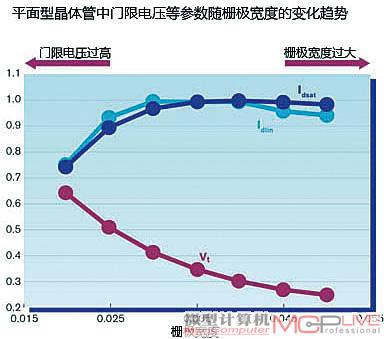
图6:图中下方Vt线为门限电压,上方两根线为管子饱和电流
和输入电流,制程越发展,工艺控制越困难。
IBM研发中心的高管Bruce Doris表示,栅极氧化物厚度减薄的速度已经很难再跟上栅极宽度缩小的步伐。而Intel公司负责制程技术的经理Mark Bohr也表示,Intel对现有结构的部分耗尽式平面型晶体管技术能否继续沿用到15nm制程节点感到“非常悲观”。
最后,其它一些传统平面型晶体管所面临的问题也将越来越难解决。工作电压的不断升高,使芯片的功耗控制变得越来越困难;而且关键尺寸的缩小还会导致漏/源极电阻的不断增大。
突破传统平面型晶体管技术瓶颈的思路和方向
目前占主流地位的思路是放弃传统的平面型晶体管技术,想办法减小沟道区的厚度,消除沟道中耗尽层底部的中性层,让沟道中的耗尽层能够填满整个沟道区—这便是所谓的全耗尽型(Fully Depleted:FD)晶体管,而传统的平面型晶体管则属于部分耗尽型(Partialiy Depleted:PD)晶体管,两者之间的区别如图7所示:
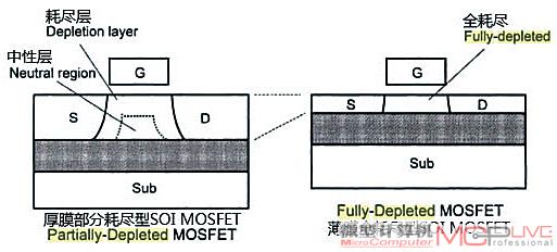
图7:中性层消失后,沟道厚度降低,进一步抑制短沟道效应,
漏电流大大降低,同时还具有具有载流子迁移率增大,
电流驱动能力提高的优势,这都为进一步降低功耗打下了扎实的基础。
不过,要制造出全耗尽型晶体管,要求沟道所处的硅层厚度极薄,这样才有可能形成全耗尽式的结构。传统的制造工艺,特别是传统基于体硅的制造工艺很难造出符合要求的结构,即便对新兴的SOI工艺而言,沟道硅层的厚度也很难控制在较薄的水平。另外一种相对较新的思路则是在晶体管的平面型工艺技术不作太大变化的条件下,转而开发全新的晶体管材料。
不论是以上哪一种方式,都要求芯片制造商转而寻求其它的晶体管结构形式或制造材料,而这也意味着业界未来一段时间内的研发重心将从应变硅和HKMG等技术转向新型晶体管结构和新材料的研制方面。
Gartner的分析师Dean Freeman为此表示,目前半导体业界所面临的情况与1980年代非常类似,当时业界为了摆脱面临的发展瓶颈,开始逐步采用CMOS技术来制造内存和逻辑芯片,从而开创了半导体业界的新纪元。
放弃传统平面型晶体管技术
围绕如何实现全耗尽型晶体管和开发新型晶体管材料这两个中心思想,以Intel/IBM为首的CPU制造厂商发展出了三种解决方案,分别是转向立体型晶体管结构,转向全耗尽型ETSOI(FD-ETSOI)技术以及转向III-V族技术,以下我们便为大家一一介绍这三种方案。
解决方案一:转向立体型晶体管结构
a.什么是立体型晶体管
立体型晶体管结构(有的材料中也称为垂直型晶体管)指的是管子的漏/源极和栅极的横截面并不位于同一平面内的技术,Intel的三门晶体管(Tri-gate)技术,以及IBM/AMD的Finfet技术均属立体型晶体管结构一类。其中Intel的三门晶体管技术尽管名字里面不含Finfet字样,但其实质仍属Finfet结构,只不过由于Intel采用的是三栅极配置的Finfet,而IBM/AMD准备的是使用双栅极配置的Finfet技术,因此为了区别于对手,同时又显示出自家技术的特色,因此便造成了两家立体结构晶体管技术命名上的区别。
图8、图9是Intel公司三门晶体管结构的原理图,栅极纵剖图以及实物放大图片:
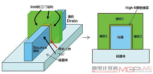
图8
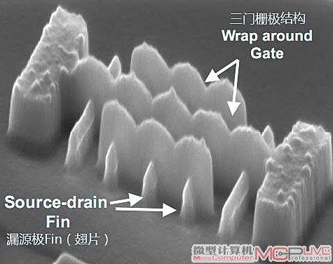
图9
IBM/AMD公司的FinFET结构则与Intel的三门结构大同小异,只不过栅极数量改为2,而且是基于SOI结构而已,其FinFET结构的纵剖图如图10。
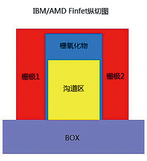
图10:注意栅极数量与Intel三门结构的区别,
以及沟道底部SOI BOX结构与体硅结构中硅基体的区别。
转向立体型晶体管结构之后,由于沟道区不再包含在体硅或SOI中,而是从这些结构中独立出来,因此可以采取蚀刻等方式制作出厚度极薄的高质量全耗尽型沟道,这样传统平面型晶体管所面临的许多问题均可迎刃而解。不过,从传统平面型与立体型晶体管的构造对比我们便可以看出,立体型晶体管所用的制造工艺与传统的平面型晶体管存在较大的差别,制造工艺的复杂程度也比后者高出许多,因此尽管有关的技术多年前便已经被提出,但要想在短时间内转向立体型晶体管技术难度是非常大的,各家在采用这种新技术之前也总是小心翼翼。接下来我们来了解一下Intel/AMD方面转向立体型结构的计划。
按Intel的脾气,他们一向对在延续平面型晶体管技术寿命方面较有优势的SOI工艺保持抗拒的态度。不过最近他们的口风不再一贯式的强硬,Intel的制程技术经理Mark Bohr表示:“我们要找的是一种性价比最高的方案,不管是SOI或者其它的什么技术,只要某种技术能够带来额外的性能提升或较低的功耗,那么我们就会采用这些技术。”而Intel前技术经理Scott Thompson预计Intel最终会选择采用三门结构晶体管制程工艺,而其它的厂商则会因为FinFET结构的制程工艺复杂性而对FinFET望而却步。
b.Intel何时转向三门技术
据Intel表示,在32nm制程的下一代22nm制程产品中,他们仍将继续采用传统基于体硅的平面型晶体管结构(此前曾有传言称 Intel会在22nm制程中转向立体结构的三门晶体管技术),他们计划于2011年年底正式推出22nm制程技术。而在2009年9月,Intel已经展示过一款采用22nm制程技术制造的SRAM芯片,这种芯片的存储密度为364Mb/inch2,内含29亿个晶体管,并且采用了Intel第三代Gate-last HKMG制程技术,栅极绝缘层和金属栅极的主要部分在制造工序的最后几个工步制造成型,避开前面的高温退火工步(45/32nm中使用的前代技术则只有金属栅极才在最后几个工步制造成型)。
至于15nm制程节点,Intel目前则正在考虑要采用哪些新的制程技术以满足要求,Intel的制程技术经理Mark Bohr表示:“全耗尽技术对降低芯片的功耗非常有效。” Intel目前正在考虑除此之外的多种可行性方案,比如是转向三门晶体管技术或者是转向全耗尽+平面型晶体管技术等等。Intel预计会在今年年中就15nm制程节点将采用哪一种新技术做出最后的决定。
c.IBM/AMD何时转向新技术
相比之下,IBM阵营方面则与Intel稍有不同,由于采用较为独特的SOI技术,加上最近他们在超薄ETSOI开发方面取得了一些进展,因此在延续平面型晶体管寿命方面具备一些得天独厚的优势。不过,出于行文流畅方面的考虑,我们准备将有关FD-ETSOI的说明放到文章的下一节阐述。这里我们可以先明确的一点是,IBM/AMD公司已经开始考虑要在22nm/15nm制程节点开始使用全耗尽型SOI技术(FD-ETSOI),不过FD-ETSOI的下一步(15nm或更高规格制程),则仍然会转向基于Finfet的立体型晶体管结构。
据AMD公司的CPU代工生产商GlobalFoundries公司的高管Pellerin表示:“在ETSOI技术发展的下一步很可能会开始启用FinFET立体型晶体管结构,两者的关系就像我们从PD-SOI过渡到FD-E TSOI那样。我看不出来ETSOI和FinFET两种技术之间存在什么矛盾之处,而且采用平面型结构ETSOI技术所能达到的晶体管密度总会出现发展瓶颈,而FinFET则可以解决这种问题。”
2.解决方案二:转向全耗尽型
ETSOI(FD-ETSOI)技术正如我们上文所介绍的那样,虽然立体型晶体管结构具有很多优点,但其制造工艺的复杂性则会令不少厂商望而却步,如果能继续延续平面型工艺的寿命,那么无论在风险还是成本方面的担忧都会大大减小。这便是IBM公司推出全耗尽型超薄SOI(FDETSOI)的目的所在。IBM 公司2009年12月份曾经展示了一种基于ETSOI(Extremely Thin SOI:超薄SOI)的22nm制程FD-ETSOI工艺,并在IEDM2009会议上展示了22nm FDETSOI晶体管制造流程图(图11):
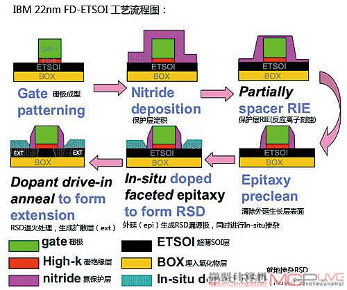
图11
IBM专家表示:“我们采用的是不会损害ETSOI层的就地掺杂技术(in-situ doping)。我们首先生成栅极隔离层;然后在漏源区用外延技术沉积生长出漏/源极,形成外延层并在漏/源极的生长过程中同时就地掺杂所需的杂质元素;此后我们会对晶体管进行加热处理,令漏源极中的掺杂原子向沟道方向扩散,形成扩散层(图11中的ext)。而加热处理过程中我们使用的尖峰退火技术(Spike Anneal)则不会对ETSOI层的结构造成不必要的损害。”那么这个如此强大的FD-ETSOI工艺,其晶体管结构是怎样的呢?
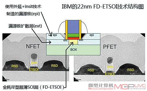
图12
如图12可见,这种22nm FDETSOI工艺的本质是将位于埋入式氧化物(BOX)上方的SOI层的厚度缩小到极低的水平,使用这种技术之后,22nm制程中的SOI层的厚度仅有6.3nm,而传统的SOI层厚度通常在 20nm以上,发展到15nm制程,SOI层的厚度还可以进一步被缩小到5nm左右。极薄的SOI层厚度保证了全耗尽设计的实现。当然,如此薄厚度的SOI层制作起来并非易事,要想将整片晶圆上的SOI层厚度控制在一定的误差水平之内,其制作难度可想而知。据IBM表示,目前由Soitec公司提供,能用于制造ETSOI产品的SOI晶圆数量仍十分有限,不过他们已经可以把这种SOI层的厚度误差控制在±5埃左右。除了对晶圆厂商提出了较高的要求之外,FD-ETSOI技术还存在其它的难点,由于SOI层的厚度极薄,因此很容易受到损坏。而且为了避免对SOI层造成损坏,在制造漏/源极时不能采用传统破坏性较强的离子注入技术,必须采用就地掺杂技术(In-situ Doping)。
隶属IBM技术同盟的GobalFoundries的技术开发经理John Pellerin表示,FD-SOI技术从应用结构上看与现有的PD-SOI技术非常相近,“我们只需要把SOI层的厚度变薄,并想办法解决ETSOI带来的一些问题即可,其它的部分则和传统的制造工艺基本相同。”当然ETSOI技术仍有许多其他的问题需要解决,比如如何减小器件的寄生电阻等。
尽管凭借FD-ETSOI技术仍可暂时延长平面型晶体管工艺的寿命,但要真正将这种技术投入实用同样需要解决很多难题,故FD-ETSOI技术仍可算得上是对传统制造技术的一次较大变革。
2.继续ETSOI的辅助技术:SiC应变硅技术
说到IBM的22nm FD-ETSOI技术,便不能不提其中采用的一种辅助型应变硅技术SiC。与我们前面提到的eSiGe类似,这也是一种应变硅技术,所不同的是eSiGe面向的对象是PMOS管中的沟道,而SiC则面向NMOS管中的沟道。
与eSiGe能为PMOS管沟道的纵向方向施加应变力的道理相反,由于C原子的体积比Si原子小,因此SiC化合物的晶格常数比Si小,这样当把SiC层嵌入NMOS管的漏源极之后,便可对沟道纵向方向施加拉伸应变力,如图13所示:

图13
IBM在描述自己的FD-ETSOI工艺时曾经提到,他们会在沉积NMOS管的漏源极时向极内掺杂碳杂质。而且另外一家IBM工艺技术联盟的成员Applied Mater ials公司也分别在IEDM2008和2009年的Semicon会展上两次强调了这种SiC应变硅技术的可行性。那么外界对SiC技术的评价如何呢?
有趣的是,Intel过去也曾经对SiC技术进行了深入的研究,不过他们现在似乎完全改变了对待SiC应变硅技术的态度,Intel过去曾经表示他们将有望使用SiC应变硅技术,不过最近Intel公司的有关人员在IEDM2009会议中接受采访时则表示不愿意就Intel在SiC应变硅技术方面取得的进展发表任何评论。而会上代表Intel做有关Intel 32nm制程技术演讲的Paul Packan则在演讲后回答记者提问的环节干脆没有理会一位记者提出的有关SiC应变硅技术在32nm制程NMOS结构中应用状况的问题。
GlobalFoundries公司的Pellerin表示:“我们正在关注SiC应变硅技术,并且正在考虑在我们的22nm制程及更高级别制程中使用这项技术。”在目前的工艺尺寸条件情况下,要想很好地控制漏源区的离子注入过程将是一项非常复杂的任务,而在IBM的FD-ETSOI工艺中,NMOS中使用的SiC应变硅技术则与PMOS中的SiGe应变硅技术一样是采用外延沉积实现的,不必再为如何控制离子注入而担忧。同时这位专家也表示:“如何在NMOS管中应用应变硅技术将是另外一个改善晶体管性能的关键技术。”
3.解决方案三:转向III-V族技术
III-V族技术是另外一种很有希望的晶体管技术发展方向,这种方案的特点是采用位于元素周期表中III-V族元素组成的材料来替代现有MOSFET管的材料,因此人们便将这种技术形象地称为“III-V族”技术,也有将采用这种技术制作的场效应管称为“QWFET”的。图14是Intel在IDEM2009会展上展示的他们在使用这种技术制造的QWFET场效应管方面取得的新进展,当时他们向这种晶体管结构中引入了High-K栅极氧化物层,这种新的High-K栅氧化物层的加入,大大减小了QWFET的漏电现象。

图14
从图14中可见,III-V族技术同样也可以在保证传统平面型晶体管制造工艺变化不大的基础上制造出关键尺寸符合发展要求的产品。
在IEDM2009会议上,来自斯坦福大学的教授Krishna Saraswat还表示,当沟道宽度降至10nm左右时,必须采用新材料来制造沟道。据他估计,业界将首先开发出NMOS管使用III-V族元素构建沟道,PMOS管使用锗元素构建沟道的技术,然后再向PMOS/NMOS统一采用III- V族元素制造沟道的方向发展。转向使用III-V族元素将大大减小器件的工作电压和管子的能耗,可将管子的工作电压减小至仅0.5V。
总结
回归到大家最关心的新制程技术在Intel/AMD产品的实际应用方面,笔者认为Intel和AMD会继续走自己的老路。其中Intel不太可能会使用ET SOI技术, IBM/GlobalFoundries/AMD则会继续将SOI发扬光大。其理由很简单,因为Intel如果采用三门晶体管技术,便可以绕开SOI。与Intel会尽可能地延长体硅制程寿命的作法截然相反的是,IBM/GlobalFoundries/AMD则会尽快转向FD-ETSOI技术,并尽全力延续FD-ETSOI的寿命。但从技术角度来分析,两者又是在统一中追求变化,都在向全耗尽型立体晶体管转变。当然,新技术的推出有时是无法按常理推测的,到底哪个方向是最正确的我们还不得而知。这就好比现在我们在不停地寻找方法或者更换交通工具,也许哪一天会去改造路面的材料甚至结构,甚至于将来的某一天去调整前进路上的空气阻力,或者突然有人告诉我们:“现在可以不走这条路了,我们发现了另一条路”,也许在陆地上,也许存在于水中、空中!在制程工艺不断发展之路上,“Intel”和“AMD”们也在不停地更换“工具”,以便让自己前进得更快、更舒服一些。
=====================================================================================
Another option is the vertical transistor. Even while the addition of many metal layers has
turned the integrated circuit into a truly three-dimensional artifact, the transistor itself is
still mostly laid out in a horizontal plane. This forces the device designer to jointly optimize
packing density and performance parameters. By rotating the device so that the drain
ends up on top, and the source at the bottom, these concerns are separated: packing density
still is dominated by horizontal dimensions, while performance issues are mostly determined
by vertical spacings (Figure 3.42). Operational devices of this type have been fabricated
with channel lengths substantially below 0.1 mm. [Eaglesham00].
Integrated circuits integrating more then one billion transistors clocked at speeds of
tens of GHz’s hence seem to be well under way. Whether this will actually happen is an
open question. Even though it might be technologically feasible, other parameters have an
equal impact on the feasibility of such an undertaking. A first doubt is if such a part can be

manufactured in an economical way. Current semiconductor plants cost over $5 billion,
and this price is expected to rise substantially with smaller feature sizes. Design considerations
also play a role. Power consumption of such a component might be prohibitive. The
growing role of interconnect parasitics might put an upper bound on performance. Finally,
system considerations might determine what level of integration is really desirable. All in
all, it is obvious that the design of semiconductor circuits still faces an exciting future.


